Peter Kinget gave a wonderful IEEE SSCS webinar on Ultra Low Voltage Analog and RF Design for nano-scale CMOS technologies yesterday. Scaling analog CMOS circuit supply voltages have been falling steadily following Moores law. Smaller transistors that have been fabricated in vast numbers has been an asset to digital circuit design. Lower supply voltages reduces power dissipation and leakage currents. The supply voltage is approaching 0.5 VDC, but it is becoming difficult to operate analog circuit on the same chip with such low voltage. Reducing the supply voltages by a factor q reduces the maximum peak-to-peak analog voltage that can be generated and this reduces the Signal to Noise Ration (SNR) by a factor of q2, for example.
![Image]()
Photo: Self-duty cycled, self-synchronized UWB Receiver SoC (65nm CMOS)
ISSCC13 Kinget Group
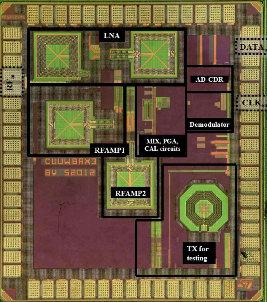
Photo: Self-duty cycled, self-synchronized UWB Receiver SoC (65nm CMOS)
ISSCC13 Kinget Group
Permalink: https://www.p-brane.com/nano/blogpost1164-Low-voltage-analog-circuits